
Science · 35 views
'Flawless on the outside, flipped within': Detecting hidden defects in 2D dielectrics with light
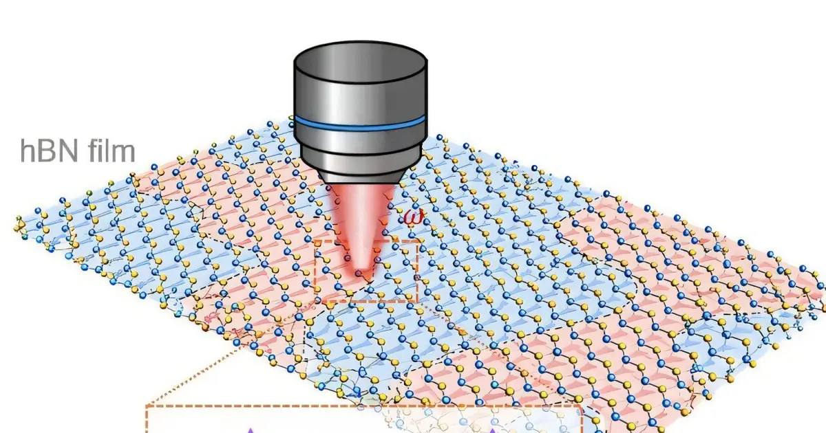
A material may appear flawless on the surface yet fail to function properly. The cause lies in structural defects hidden within two-dimensional thin films, which are considered key materials for next-generation semiconductor devices.

AI Summary
Researchers have developed a method to detect hidden defects within two-dimensional thin films using light. This breakthrough is significant because it addresses a common issue with these materials, which can appear flawless on the surface but fail to function properly due to internal defects. The method's ability to identify these invisible flaws could improve the reliability of next-generation semiconductor devices. The development of this optical analysis technique is a step forward in understanding and characterizing the properties of 2D dielectrics, which are crucial components in emerging technologies.
AI summaries can be wrong sometimes—always verify important details using the source article.
How AI & Automation are usedCoverage Context
More from Science
Continue reading recent Science coverage
- Plasma and electricity convert CO₂ into methanol, butane and other useful chemicalsContinue reading
- History is being rewritten at an archaeological site in Morocco. What the discovery of an ancient wall tells usContinue reading
- 'Living Medication' May Have Restored Bone Strength in 10 Patients With Advanced OsteoporosisContinue reading
- What are best options for controlling GSL dust, and what would they cost?Continue reading
Support HappeningNow
Independent AI-powered news analysis is reader-supported. Your contribution helps cover infrastructure, summaries, and continued platform development.
Support HappeningNow